반도체 신기술: 포토닉 인터포저칩
A New Semiconductor Technology: Photonic Interposer Chips
- 저자
-
박상기지능형부품센서연구실 sahnggi@etri.re.kr
- 권호
- 40권 4호 (통권 215)
- 논문구분
- 일반논문
- 페이지
- 113-123
- 발행일자
- 2025.08.01
- DOI
- 10.22648/ETRI.2025.J.400411
 본 저작물은 공공누리 제4유형: 출처표시 + 상업적이용금지 + 변경금지 조건에 따라 이용할 수 있습니다.
- 초록
- Photonic interposer chips are expected to drive the emergence of a new semiconductor market by offering considerably higher bandwidths than high-bandwidth memories. Based on the current distribution of light sources deployed in data centers, vertical-cavity surface-emitting lasers (VCSELs) are regarded as promising light sources for integration into photonic interposer chips. Accordingly, it is essential to develop technologies that enable the efficient coupling of VCSEL light into and out of optical waveguides. Since 2023, TSMC, Samsung,and other leading companies have invested substantial human and financial resources in silicon photonics. However, the potential of VCSEL-based photonic interposer chips has not been fully recognized. If the coupling technology can be secured, VCSEL-based photonic interposer chips could be the most viable solution for commercialization. Because the first demonstration product provides a competitive edge, it is crucial for companies to implement timely strategic initiatives.
Share
I. 서론
반도체의 기술 경쟁은 공정기술과 설계기술, 그리고 새로운 기술의 경쟁으로 진행되고 있다. 공정기술은 3차원 구조의 게이트(GAA: Gate All Around)와 2nm 이하 선폭을 대량생산에 적용하는 시점(2025년)에 있다. 선폭을 최소화하면 소자의 밀도를 높이는 것뿐만 아니라 성능을 향상시키는 효과를 동시에 얻는다. AMD와 NVIDIA는 초기부터 TSMC에 제작을 위탁함으로써 CPU와 GPU의 최고 성능을 확보한 데 반해, 자사 Fab을 고수해온 Intel은 오랫동안 업계 최고의 설계기술을 보유하였지만 궁극적으로 고전을 면치 못한 계기가 되었다.
대기업들의 판도를 재편할 수 있는 새로운 기술은 AI 칩과 포토닉스 기술을 들 수 있다. GPU를 포함한 AI 칩은 설계기술과 파운더리 기술이 핵심이고, 이미 NVIDIA와 TSMC를 선두로 판도가 고착화되어 가고 있다. 포토닉스 기술은 광소자 기술과 2.5D & 3D 패키징 기술이 핵심이고, 10nm 이하급 파운더리 기술이 요구되지 않기 때문에 미국, 유럽뿐만 아니라 중국도 초기부터 많은 투자를 한 분야이다. TSMC를 포함한 타이완 기업들은 인터포저칩 제작과 첨단 패키징 기술을 선도하고 있으며, 2023년부터 각종 발표를 통해 실리콘 포토닉스 기술에 인력과 자금을 집중하고 있다[1]. 이에 삼성전자도 2024년 6월 실리콘포토닉스 기술의 상용화 일정을 발표한 바 있다[2].
고대역폭 메모리(HBM: High Bandwidth Memory)는 2013년 SK-하이닉스가 최초로 상용화하였고, 2015년 AMD사의 GPU에 처음 사용되었다[3,4]. AMD 사는 메모리와 GPU 간 고대역폭 통신을 구현하기 위해 UMC, ASE, 그리고 SK-하이닉스와 4자 간 컨소시엄을 구성하여 GPU 패키지 모듈을 상용화하였다. 2016년 삼성전자도 HBM2를 상용화하였고, NVIDIA는 TSMC와 삼성전자 제품을 이용하여 GPU 모듈(모델명 P100)을 출시하였다[3]. 2019년까지 시장이 부진한 사이 삼성전자는 HBM 제품생산을 중단하였고, NVIDIA는 TSMC와 SK-하이닉스 제품을 사용하여 본격적인 시장을 열었다. 최근 DRAM 시장 점유율에서 SK-하이닉스가 최초로 선두를 차지했다는 보도가 있었다. 이는 새로운 기술이 기업의 판도를 바꾸는 대표적인 예이다.
포토닉스 반도체는 기업들의 위상을 한 번 더 재편할 전망이다. 2024년 TSMC가 발표한 자료에 따르면 포토닉스 기술은 단계적으로 반도체칩에 도입될 예정이고, 이 경우 통신속도는 약 10배 빨라지고 전력소모는 약 10배 감소하는 결과를 예측하였다[5]. 이를 근거로 타이완은 TSMC를 필두로 30개 기업이 연합체를 결성하여 실리콘포토닉스 기술에 몰두하고 있다[6].
미국의 반도체 기업들(Intel, HP, IBM 등)은 2000년대 초반부터 지속적인 투자와 연구를 진행하여 포토닉스 기술을 선도하고 있다. Intel은 실리콘포토닉스 기술을 활용한 데이터센터용 광송수신기를 최초로 상용화하였고, 현재까지 수백만 개의 누적판매 기록이 있다. 또한, 표면방출레이저(VCSEL: Vertical Cavity Surface Emitting Laser) 기반의 포토닉스 연구도 매년 우수한 논문을 발표하고 있다[7]. HP사는 실리콘포토닉스 연구를 늦게 시작하였지만, 최근 우수한 논문을 발표하고 있다[8]. 특히 단일모드 VCSEL에 대해 최고 수준의 특성을 보고한 바 있다[9]. IBM사는 실리콘포토닉스 연구를 2010년대 중반 중단하였지만 표면방출레이저 기반의 포토닉스 연구는 미국 정부의 지원과 함께 꾸준히 수행하고 있으며, 최근 우수한 특성을 보고하였고 표준화 작업도 선도하고 있다[10].
일본은 실리콘포토닉스 연구에 대해 뚜렷한 연구 논문을 찾아볼 수 없을 만큼 미온적이었다. 그러나 표면방출레이저 기반의 광소자 연구는 최고 특성의 논문을 보고한 바 있다[11]. 특히 동경공업대학교에서 연구한 단일모드 표면방출레이저의 특성은 세계 최고 수준에 있다[12]. 후지쓰사와 후라가와사는 일본 정부로부터 과제를 수주하여 동경공업대학교의 단일모드 표면방출레이저를 이용한 다채널 광송수신기 제작을 진행하고 있다[13,14].
II. 포토닉스 기술
표 1은 반도체 업계에서 예측하는 기술 트렌드를 나타내고 있다[5]. 2024년을 기준으로 서버 보드 끝에 광송수신기를 플러그형으로 꽂는 방식에서 2026년에 패키지 기판에 컴퓨터칩과 함께 패키지하는 방식(CPO: Co-Packaged Optics)으로 진화하고, 최종적으로는 실리콘칩 위에 다른 컴퓨터칩과 함께 패키지하는 방식으로 진화한다. 하나의 광송수신기는 현재 1.6Tb/s의 데이터를 전송하지만 단계적으로 10배 증가할 예정이다. 그리고 기가비트당 전력소모는 약 10배 감소하고 전송 측에서 수신 측까지 전송하는 데 걸리는 시간은 약 20배 감소한다.
표 1 광트랜시버 기술 트렌드
| Pluggable on Board 2024 | CPO on Substrate 2026 | CPO on Chip 202x | |
|---|---|---|---|
| Bandwidth | 1.6Tb/s | 6.4Tb/s | 12.8Tb/s |
| Power | 1x | < 0.5x | < 0.1x |
| Latency | 1x | < 0.1x | < 0.05x |
그림 1은 데이터 센터의 서버와 스위치 장비가 랙(Rack)에 배치되는 그림을 나타낸다. 하나의 랙에는 통상 10~30개의 서버가 있고, 맨 위 칸에는 대개 스위치 장비가 있다. 대규모 데이터 센터는 이러한 랙이 수천 개 배치되어 있다. 서버와 스위치, 그리고 스위치와 다른 스위치 간에는 광통신 케이블로 연결되어 있다. 다만, 거리 10m 이내에서는 구리선 케이블이 사용되기도 한다. 그림에 표시된 바와 같이 500m보다 먼 거리의 스위치 간에는 DFB(Distributed Feedback Laser) 레이저와 단일모드 광섬유(SMF: Single Mode Fiber)를 사용하고, 나머지는 대부분 표면 방출레이저와 멀티모드 광섬유(MMF: Multi-Mode Fiber)를 사용한다.

표 2는 실리콘포토닉스 기술과 표면방출레이저 기반 광트랜시버 기술을 비교하였다. 데이터 센터 내 통신거리는 대부분 100m보다 짧으므로 주력 광원은 표면방출레이저이다. 실리콘포토닉스 기술은 100m보다 긴 거리의 통신에서 일정 부분 활용되고 있으나 기존 광통신에 사용되는 광트랜시버가 주로 사용되고 있다. 실리콘포토닉스 광트랜시버는 상대적으로 전력소모가 크고 제작비용이 표면방출 레이저 기반 광트랜시버보다 높다. 광소자의 채널당 면적은 표면방출레이저를 기준으로 실리콘포토닉스 광원이 대략 5배 크다. 이는 광변조기(실리콘광도파로의 마하젠더 변조기를 주로 사용함)가 차지하는 면적에 기인한다. 실리콘포토닉스 광트랜시버는 DFB 레이저와 단일 모드 광섬유를 사용하기 때문에 500m, 2km, 10km의 거리에 주로 사용된다.
표 2 실리콘포토닉스와 표면방출레이저 기반 광트랜시버 비교
그림 2(a)는 플러그형 광송수신기(OE: Optical Engine)가 스위치와 서버에 결합되는 구조를 나타낸다. 최근 데이터 센터에 사용되는 스위치칩(ASIC)의 신호처리 속도는 51.2Tb/s이다. 광송수신기 32개가 마더보드 끝에 있는 플러그형 단자에 꽂혀 있다. 16개는 입력 단자이고, 나머지 16개는 출력 단자이다. 16개 채널(채널당 1.6Tb/s)에서 총 25.6Tb/s의 데이터가 입력되면 정해진 명령에 따라 채널을 바꾸어 25.6Tb/s의 데이터가 출력된다. 서버에는 광송수신기 1개가 마더보드 끝에 있는 플러그 단자에 꽂혀 있다. CPU, 메모리, GPU는 마더보드의 전기회로로 연결되어 있다. 고가의 GPU는 2.5D 패키지 기술을 사용하여 실리콘 인터포저칩 위에 HBM과 함께 집적되어 있다.
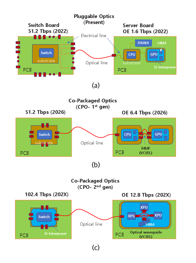
그림 2(b)는 광송수신기가 마더보드 끝에서 스위치칩 또는 CPU칩의 기판(Package Substrate)으로 옮겨진 모습을 나타내고 있다. 단순히 위치만 옮기는 것이 아니라 스위치칩 또는 CPU칩과 함께 패키징된다. 광송수신기의 데이터 처리는 6.4Tb/s가 예상되고 2026년경 상용제품이 출시될 것으로 예측된다. 그림 2(c)는 광송수신기가 실리콘 인터포저칩 위에 스위치칩 또는 CPU칩과 함께 집적되는 모습을 나타낸다. 마더보드 끝에서 기판 끝으로, 그리고 실리콘 인터포저칩 끝으로 옮김으로써 성능변화는 표 1에 나타낸 바와 같다.
그림 3은 광송수신기가 마더보드 끝단에 위치하는 것과 기판 또는 실리콘 인터포저칩 위에 위치할 때 변화하는 기술적 차이를 설명한다. 즉, 차이점은 DSP(Digital Signal Processor) 소자가 하나 없어진다. 이는 데이터 전송이 2회에서 1회 전송으로 단축됨을 의미한다. 그림 3(a)를 참고하면 스위치 또는 CPU에서 나온 데이터 신호는 DSP 1에 전달된다. 다수의 신호처리 과정을 거치지만 가장 중요한 처리는 직렬화(Serialize), 역직렬화(Deserialize)이다. 데이터가 전송되는 단계마다 회선 수가 다르므로 서로 병합하거나 나누어서 전송한다. 마더보드를 통과하기 위해 데이터신호는 DSP 1에서 직렬화하고 DSP 2에 역직렬화를 한 후 다수의 처리과정을 거쳐서 신호를 재생한다. 재생된 신호는 광신호로 변환되기 전에 다시 광통신의 회선 수에 맞게 직렬화한다. 직렬화된 신호는 변조기 드라이버(Driver)로 보내지고 변조기를 작동하기에 적당한 크기로 증폭된다. 증폭된 신호는 변조기에 전달되어 광신호로 변환된다. 광송수신기에는 전자칩(EIC)과 포토닉칩(PIC)이 접합되어 있고 DSP 2는 EIC에 내장되어 있다. 광신호를 수신할 때는 동일한 단계의 역순을 거쳐서 스위치칩 또는 CPU에 전달된다.

그림 3(b)는 광송수신기의 EIC와 PIC가 DSP 1 위치로 이동되는 점을 나타낸다. 스위치칩 또는 CPU에서 나온 데이터는 단 한 번의 직렬화를 거친 후 변조기 드라이버로 보내져서 광신호로 변환된다. 이 경우 전력소모와 전송시간에서 큰 이득을 갖게 된다. 또한, 회선 수를 크게 높일 수 있어 데이터 전송량(Bandwidth)도 비례하여 높일 수 있다. 코패키지 옵틱스(CPO)라 불리며 2026년경 상용화될 예정이다. 단점은 광송수신기가 고장 날 경우 고가의 스위치칩 또는 CPU칩과 별개로 교체할 수 없는 점이다.
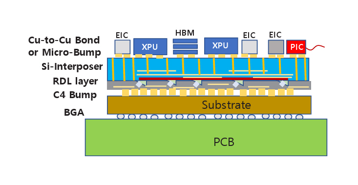
그림 2(c) 또는 그림 3(b)에 대한 수직 구조를 그림 4에 나타내었다. 포토닉 인터포저에 적용되는 기술에 따라 차이가 있을 수 있으나 대표적으로 예상되는 구조이다. 실리콘 인터포저칩 위에 CPU, HBM, EIC와 같은 전자소자를 접합한다. 최신 기술인 하이브리드 본딩(Cu-to-Cu Hybrid Bonding) 기술을 적용할 수 있다. 실리콘 인터포저칩 아랫면에는 전기 회로뿐만 아니라 광도파로를 형성하고 광소자들이 배치된다. 실리콘 관통전극(TSV: Through Silicon Via)에 의해 윗면과 아랫면의 전기회로는 연결된다. 광도파로와 광소자 아래에는 RDL(Redistribution Layer)이 형성되고 RDL의 회로가 패키지 기판(Substrate)과 전기적으로 연결된다. 외부로 광신호를 전달하기 위해 그림 3(b)의 OE(Optical Engine) 부분을 실리콘 인터포저 윗면에 그림 4의 PIC와 같이 배치할 수 있다.
III. 표면방출레이저 기반 포토닉스
2025년 현재 코패키지 옵틱스에 사용될 수 있는 가장 높은 특성을 보고한 광변조기들을 표 3에 나타내었다. 표면방출레이저를 제외한 나머지는 실리콘포토닉스 광트랜시버에 사용되는 변조기들이다. 학회발표보다 비교적 신뢰성이 높은 저널 논문을 근거로 하였다. 3dB 밴드폭(Bandwidth)은 변조기의 중요한 특성 중 하나이다. 신호의 세기를 변조속도의 함수로 관측할 때 특정 성분의 신호 세기가 1/2로 떨어지는 지점의 변조속도이다. 직접 변조 레이저(DML: Directly Modulated Laser)가 가장 높은 값을 나타내고 있다. 단점은 전력소모가 크다는 점이다. 이는 변조속도를 최대로 높이기 위해 반사거울(DBR: Distributed Brag Reflector)의 파장을 레이저형광 곡선의 꼭지점이 아닌 옆면에 맞추었기 때문이다. 즉, 변조속도를 높이기 위해 출력파워를 상당 부분 희생시킨 것이다. 변조속도를 높이기 위해 다른 변조기들도 다양한 방법으로 타협점을 찾는다.
표 3 광변조기의 최고 특성
| Si M-Z 변조기 | Si 링변조기 | |
|---|---|---|
| 3dB 밴드폭 변조속도 (PAM4) | 47GHz | 49GHz |
| 250Gb/s | 200Gb/s | |
| 소속 논문 | 캐나다, Mcgill U. PTL 2021[17] | 미국, HP사 Nature comm. 2024[18] |
| EML/DML | VCSEL | |
| 3dB 밴드폭 변조속도 (PAM4) | EML-65GHz | 멀티모드 30GHz |
| 225Gb/s | 224Gb/s | |
| DML-108GHz | 단일모드 39.4GHz | |
| 256Gb/s | 100Gb/s | |
| 소속 논문 | 일본, Mitsubishi, JLT 2024 [19] | 독일, VIS EL 2024[21] |
| 일본 NTT Nature Photon 2021[20] | 일본, 동경공업대 CLEO 2024[12] |
전기흡수 변조 레이저(EML: Electro-Absorption Modulated Laser)도 변조기의 흡수파장 위치를 변조속도에 유리하게 맞춘다. 이를 위해 레이저와 변조기에 사용되는 양자우물층(Quantum Well Layers)을 서로 다르게 설계하여야 한다. 이는 출력뿐만 아니라 제작에도 불리하게 작용하기 때문에 많은 연구 그룹이 변조속도가 더 빠름에도 불구하고 EML/DML을 선택하지 않고 마하젠더 또는 링 변조기를 사용한다. 최근 대부분의 전송실험은 4단계 진폭 변조(PAM4: Pulse Amplitude Modulation 4) 기술을 사용한다. 기존의 on-off 변조는 2단계 진폭 변조에 해당한다.
표 3에 나타난 바와 같이 대부분의 변조기는 200Gb/s 이상의 변조속도를 보고하였다. 따라서 변조속도는 변조기 선택의 큰 변수가 아님을 알 수 있다. 다만 단일모드 VCSEL은 더 많은 전송실험이 필요할 것으로 보인다.
표 4는 각 변조기별로 광송수신기 제작에 대한 정보를 나타낸다. 실리콘 마하젠더 변조기와 EML/DML 레이저를 이용하여 그림 3의 코패키지 옵틱스를 위한 설계와 PIC, EIC까지 제공한다는 벤처 기업들은 상당히 많이 있다. 표 4에 제시된 기업은 일부 대표적인 기업들이다. 실리콘링 변조기를 이용한 광트랜시버는 Intel이 오랜 기간 준비해 왔고, 최근 논문을 발표하기도 하였다[15]. 그러나 다른 기업은 확인되지 않는다. 표면방출레이저를 이용한 코패키지용 광트랜시버는 다수의 기업이 준비하고 있지만[7,10,13,14], 포토닉 인터포저칩의 광도파로에 대한 입출력 기술을 보유한 기업은 (주)오프로세서(OPROCESSOR INC)가 유일하다[16].
표 4 포토닉 인터포저 칩의 구성요소 및 특징
표면방출레이저는 프리즘 위에 광원, 변조기, MUX/DeMUX가 동일한 위치에 놓이기 때문에 차지하는 면적은 광원과 포토다이오드(PD: Photodiode)의 면적이다[16]. 프리즘은 표면방출레이저와 비슷한 크기로 만들 수 있다. 다른 방식들은 구성요소들이 평면으로 나열되기 때문에 구성요소 각각이 면적을 차지하게 된다. 표면방출레이저를 기준으로 채널당 면적과 전력소모를 비교하면 2~8배, 5~10배 높은 크기가 필요하다. 또한, 소자 제작에 요구되는 원가도 표면방출레이저가 가장 낮다. 따라서 표면방출레이저 방식이 포토닉 인터포저칩 제작에 가장 유리할 뿐만 아니라 실현성이 높다. 나머지 방식은 그림 3(b)에서 실리콘 인터포저칩 끝에 있는 광트랜시버가 상용화 한계일 가능성이 높다. 특히 마하젠더 방식과 EML/DML 방식은 채널당 면적이 크기 때문에 포토닉 인터포저칩에 적용될 가능성이 작다.
실리콘 링변조기 방식의 경우 면적과 전력소모를 수용한다고 하여도 수율과 온도 컨트롤 문제를 간과할 수 없다. 양자우물층이 형성된 화합물 웨이퍼(InP wafer)를 반사거울(DBR)이 새겨진 실리콘 웨이퍼에 접합하여 레이저(DFB Laser)를 만들기 때문에 광학적 정렬과 대량생산에 유리하다는 점이 Intel에서 강조하는 링변조기 방식의 강점이다. Intel과 OpenLight 등 일부 회사는 동일한 방법으로 제작한 레이저를 마하젠더 변조기에도 광원으로 사용하고 있다. 그러나 단점은 수율이 매우 높아야 한다는 점이다. 개별 광송수신기 제작에는 수율이 문제되지 않는다. 양호한 칩을 선택하여 사용할 수 있기 때문이다. 그러나 포토닉 인터포저칩에 사용되기 위해서는 수십~수백 개의 레이저가 모두 양호해야 하므로 수율이 문제될 수 있다. 파장이 다를 경우 양자우물(Quantum Wells)의 설계가 달라지므로 다수의 파장을 사용할 때 각 파장별 레이저를 모두 다른 조각 웨이퍼로 접합해야 한다. 접합하는 웨이퍼 조각의 개수와 난이도가 높아진다. 그리고 제작한 레이저가 적합한가에 대한 판정은 포토다이오드를 다 제작한 후 양호한 포토다이오드를 통해서만 확인할 수 있고 부적합한 레이저는 교체할 수 없다. 즉, 단 몇 개의 부적합 레이저로 인해 포토닉 인터포저칩 전체를 버릴 수 있다.
실리콘 링공진기를 변조기로 사용하기 위해서는 링의 공진파장이 레이저 파장과 일치해야 한다. 제작과정의 통계적 편차로 인해 공진파장이 레이저 파장과 통상 일치하지 않는다. 따라서 링 변조기 표면에 마이크로 히터를 설치하고 국부적으로 온도를 올려서 파장을 일치시킨다. 주변 온도가 변화하면 파장이 다시 불일치하게 되고 이를 상시적으로 모니터링하여 파장을 일치시켜야 한다. 이러한 피드백 시스템을 수십~수백 개의 변조기마다 모두 독립적으로 설치하여 운영하는 것은 기술적으로도 어렵지만 큰 원가 상승을 초래할 수 있다.
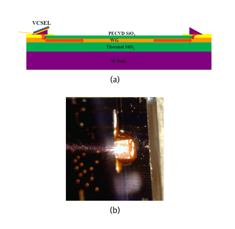
표면방출레이저(VCSEL)의 최대 장점은 빛이 표면에 수직하여 나오므로 웨이퍼를 칩으로 절단하지 않고 웨이퍼 상태에서 레이저를 판정할 수 있는 점이다. 이 점은 표면방출레이저를 이용한 포토닉 인터포저칩 제작에도 동일하게 적용된다. 그림 5는 참고문헌 [16]에 제시된 표면방출레이저 신호의 광도파로에 대한 전송 실험을 나타낸다.
그림 5
광도파로에 대한 표면방출레이저 신호 전송 실험
출처 Reprinted from S.G. Park et al., “Technologies for optically interconnected CPU,” TechRxiv, 2022. doi: 10.36227/techrxiv.19738048.v1.

그림 5(a)는 프리즘을 통해 표면방출레이저 신호를 광도파로에 입출력시키는 구도를 도식적으로 나타내고 있다. 그림 5(b)는 프리즘 표면에 레이저 빛이 방출되는 모습을 찍은 사진이다. 참고문헌 [16]은 접속손실과 전송손실이 포토닉 인터포저칩에 적용할 수 있는 범위에 있음을 증명하고 있다.
다수의 연구그룹이 표면방출레이저 빛을 실리콘 물질의 광도파로에 입출력시키는 실험결과를 발표하였다[22-24]. 실리콘 광도파로는 굴절률이 커서(굴절률 3.45) 프리즘을 사용할 수 없고 회절격자(Grating)를 사용하여야 한다. 표면방출레이저는 무편광인데 반해 회절격자는 TE 모드만 적절한 각도로 회절되고 TM 모드는 회절되지 않아 기본적으로 3dB 접속손실이 발생한다. 상용제품의 마이크로렌즈를 사용하면 부피가 지나치게 크므로 사용할 수 없고, 따라서 레이저 빛과 도파로 간 모드 크기가 맞지 않아 논문들은 10dB 이상의 접속손실을 보고하였다.
실리콘 광도파로는 통과하는 광신호의 전파손실(Propagation Loss)이 큰(1~3dB) 단점이 있다. 또한, SOI(Silicon on Insulator) 웨이퍼를 사용하여야 한다. 그리고 광도파로가 각종 로직 소자와 같은 실리콘 층을 사용하여야 하므로 회로 설계의 단점을 감수하여야 한다.
실리콘 팹에서 제공하는 공정을 사용하지만 실리콘이 아닌 물질(SiO2, Si3N4 등)을 이용하여 광도파로를 제작하는 것이 유리하다. ETRI 연구원과 창업 기업은 이러한 물질을 이용하여 제작한 광도파로에 표면방출레이저 신호를 입출력시키는 기술과 실험 결과, 그리고 지식재산권을 참고문헌 [16,28]에 나타내었다.
표면방출레이저를 이용한 포토닉 인터포저칩은 웨이퍼 상태에서 광신호의 입출력 검사가 가능하므로 대량생산에 매우 유리하다. 먼저 프리즘을 정해진 위치에 항구적으로 접합한다. 그리고 양호한 표면방출레이저를 선택하여 홀더 장비에 올린다. 홀더 장비는 전류를 인가하여 실시간으로 레이저 빛이 나오는 모습을 관찰할 수 있도록 전극을 구성한다. 표면방출레이저를 해당 위치에 접근시키고 반대편 프리즘에서 빛이 나오는 상태를 실시간으로 관측한다. 가장 양호한 상태에서 약 120℃에서 액체화되는 투명접착제를 이용하여 임시로 접합한다.
대량생산을 위해 한 번에 수십~수백 개를 동시에 접합하고 불량한 것은 교체하거나 수정할 수 있다. 포토닉 인터포저칩에서 모든 프리즘과 표면방출레이저, 그리고 포토다이오드는 위치가 정해져 있으므로 다수의 마스크칩을 만들어 해당 위치에 위 소자들을 미리 정렬시켜 놓는다. 실제 칩이 준비되면 홀딩 장비로 한 번에 옮겨 칩에 접합할 수 있다. 임시로 접합한 후에도 표면방출레이저와 포토다이오드는 상태를 확인하여 불량한 것은 해당 소자와 프리즘만을 120℃까지 열을 가하여 교체할 수 있다. 모든 표면방출레이저와 포토다이오드가 양호한 상태임이 확인되면 RDL 몰딩 과정에서 영구적인 접합을 한다.
IV. 논의
직접 변조하는 표면방출레이저의 빛을 광도파로에 입출력하고 다수의 파장을 하나의 광도파로 전송하는 기능이 가능하게 되면 실리콘 칩상에서 네트워크를 구성할 수 있다. 또한, 광신호 생성부터 회로 구성까지 가능하므로 표면방출레이저 기반 포토닉스가 가능하게 된다. 참고문헌 [16]은 하나의 채널에 대해 입출력 실험 결과를 보고하였지만 N개의 채널은 단순 반복이므로 채널 수에 구애받지 않는다. 따라서 그림 4에 나타낸 몇 개의 XPU와 HBM을 연결하는 포토닉 인터포저칩뿐만 아니라 그림 6과 같이 수십 개의 연산칩과 메모리칩을 연결하는 광네트워크칩도 가능함을 나타낸다. 따라서 표면방출레이저 기반 포토닉스칩은 발전 가능성이 높다고 할 수 있다.
그림 6
광네트워크칩(Optical Network Chip) 모형도
출처 Reprinted from S.G. Park et al., “Technologies for optically interconnected CPU,” TechRxiv, 2022. doi: 10.36227/techrxiv.19738048.v1.

그림 2(c)에서 칩 외부에 12.8Tb/s의 통신량을 공급하기 위해서는 칩 내부 통신량도 더 크거나 최소한 같은 양을 공급해야 한다. 2024년 JEDEC 표준에 의해 HBM4와 GPU 간 통신량(Bandwidth)은 13.1Tb/s이다[3]. JEDEC 표준에 의해 HBM3E와 HBM4의 전기배선은 래인당(per Lane, 한 래인은 두 개의 전선으로 구성) 각각 9.8Gb/s, 6.4Gb/s를 규정하고 있다[3]. 2022년 802.3db에 의해 광신호는 채널당 106.25Gb/s를 규정하고 있으며, 200Gb/s 규정도 진행하고 있다[25,26]. 표 3에 나타낸 바와 같이 거의 모든 광변조기는 200Gb/s의 통신속도를 발생시킬 수 있다. 파장다중(Multiplexing)을 통해 하나의 광도파로가 8개 주파수를 수용할 경우[10] 광도파로는 전기선에 비해 최소 160배 이상 큰 통신량을 수용한다. 12.8Tb/s의 통신량을 기준으로 전기신호는 2,560개(1,280Lanes)의 전선을 배치하여야 하지만 광신호는 16개(채널당 2개 주파수 사용, 총 64채널, 광도파로 하나에 4개 채널 수용)의 광도파로만 배치하면 된다. 즉, 광신호를 도입하지 않고 전기배선만 사용하면 머지않아 인터포저칩 내에 수용할 수 없을 만큼 전선의 수가 증가하게 됨을 예측할 수 있다.
전기신호는 1Gb/s당 > 1mW 전력을 소모하지만, 광신호는 1Gb/s당 < 0.1mW 전력을 소모한다[27]. 전기신호는 일정 거리마다 신호를 재생하여야 하지만 광신호는 충분히 먼 거리에도 재생이 요구되지 않는다. 따라서 광신호는 전력소모와 통신시간(Latency)에서 수십 배의 이득을 얻게 된다. 또한, 전기신호는 전선들을 가까이 배치할 경우 Gb/s 이상의 고속신호에 대해 상호간섭(Cross Talk)이 발생하므로 전선 간 거리를 좁히는 데 한계가 있지만, 광신호는 상호간섭이 발생하지 않는다. 이와 같은 이점으로 인해 2000년대 초반부터 반도체칩 내 광신호 도입의 필요성이 제기되어 왔다.
표 4에 나타난 바와 같이 채널당 면적, 전력소모, 제작비용(Cost), 광소자에 대한 웨이퍼 단계의 테스트 가능성 등을 고려하면 표면방출레이저가 포토닉 인터포저칩 제작에 가장 유리하다. 실리콘 광도파로 기반의 변조기 방식은 그 단점들로 인해 기존의 인터포저칩 끝에 광트랜시버를 코패키지하는 단계가 한계일 가능성이 높다. 이 경우 시장 또한 현재와 같이 광트랜시버 시장 규모와 큰 차이가 없게 된다. 그리고 타이완 기업들의 독점 시장이 그대로 유지될 가능성이 높다. 포토닉 인터포저칩의 상용화까지 도달하여야만 새로운 반도체칩 시장이 열릴 뿐만 아니라 광도파로에 대한 입출력 기술을 보유한 기업들에 유리한 기회가 있다.
포토닉 인터포저칩의 시장규모는 HBM 시장규모에 견주어 추정해 볼 수 있다. 왜냐하면 HBM이 인터포저칩 위에 집적되어 늘 함께 공급되기 때문이다. 12.8Tb/s의 통신량을 기준으로 200Gb/s용 표면방출레이저와 포토다이오드가 각각 최소 64개 이상 필요하게 된다. 현재 가격을 기준으로 비교하면 광소자들의 가격이 HBM 가격보다 수십 배 크다. 따라서 포토닉 인터포저칩은 최소한 HBM보다 시장규모가 클 것임을 예측할 수 있다. 그리고 전기배선으로 통신량을 감당할 수 없는 시점부터 단계적으로 광신호가 도입될 가능성이 높다. 표면방출레이저와 포토다이오드는 제작원가가 낮으므로 대규모 수요가 발생할 경우 광소자의 총 가격도 현재 계산보다 크게 떨어질 것이다. 가장 먼저 데모 제품을 출시하고 시장을 개척하는 회사에 유리한 시장 조건이 형성될 가능성이 높다.
V. 결론
HBM은 XPU-to-Memory 대역폭만 확장하지만 포토닉 인터포저칩은 XPU-to-XPU, XPU-to-Memory 간 대역폭을 확장시킨다. 따라서 포토닉 인터포저칩은 HBM에 이어 고대역폭을 제공하는 새로운 반도체칩 시장을 창출할 것으로 전망된다. 표면방출레이저는 포토닉 인터포저칩에 사용될 가장 유력한 광원이다. 광도파로에 멀티모드 표면방출레이저 신호를 입출력할 수 있는 기술은 실험결과, 지식재산과 함께 한국전자통신연구원 연구원과 창업기업이 전 세계에서 유일하게 보고한 바 있다[16,28].
현재 GPU 패키지에서 실리콘 인터포저칩은 타이완 기업이 독점하고 있다. 타이완은 포토닉스가 도입되어도 우위를 계속 유지하기 위해 다른 나라보다 훨씬 빠르게 움직이고 있다. 전술한 바와 같이 표면방출레이저 방식이 유력하므로 입출력 기술을 확보한 기업에 충분히 승산이 있다. 반도체 대기업은 물론 패키지 분야 중견기업도 도전할 수 있는 기술이다.
파운더리 공정기술 또는 XPU 칩 설계기술에서 세계 최고가 아니면 경쟁력을 신기술에서 찾아야 한다. HBM을 개척한 기업은 창사 이래 처음으로 메모리 분야 1위에 올라서고 있다. 아무리 장기간 1등이었어도 개발부터 시장 개척까지 신기술을 스스로 완수하지 못한 기업은 더 이상 그 위치를 유지하지 못하는 환경이다. 특히 연구개발 단계의 위험을 감수하지 않고 타사가 상용화하여 개척한 시장을 늦게 도전하여 1등이 되는 시대는 지났다. 표면방출레이저 기반 포토닉 인터포저칩은 분명 도전할 만한 신기술 기회라고 할 수 있다.
I. Introduction
Technological competition in the semiconductor field has been driven by advancements in process and design technologies and the development of new technologies. In process technology, the industry is approaching the mass production stage (2025) of sub-2nm node and 3D gate structures such as Gate-All-Around (GAA). Minimizing feature size not only increases transistor density but also enhances performance. AMD and Nvidia secured top-tier performance in CPUs and GPUs early on by outsourcing to TSMC. By contrast, Intel’s commitment to in-house fabrication has multicontributed to its difficulties in competing with more flexible rivals, despite having led in design technology for years.
Artificial intelligence (AI) accelerators and photonics represent disruptive new technologies with the potential to alter the semiconductor industry landscape. AI chips, including GPUs, depend heavily on advanced design methodologies and cutting-edge foundry capabilities. This domain is becoming consolidated by Nvidia and TSMC. Photonic integration, on the other hand, leverages optical components and advanced 2.5D/3D packaging. Since it doesn’t require sub-10nm lithography, China has also been investing in it from the beginning, along with the U.S. and Europe. Taiwanese firms, particularly TSMC, have been at the front of interposer chip fabrication and 2.5D/3D packaging, and have started R&D and investments toward silicon photonics since 2023 [1]. Samsung also announced roadmap for commercialization of silicon photonics in June 2024 [2].
High Bandwidth Memory (HBM) was first commercialized by SK Hynix in 2013 and was initially adopted in AMD’s GPUs in 2015 [3,4]. To enable high-bandwidth communication between memory and GPU, AMD formed a four-party consortium with UMC, ASE, and SK Hynix, leading to the successful commercialization of the GPU packaged with HBM. In 2016, Samsung Electronics introduced HBM2, and Nvidia released P100 GPU using TSMC’s foundry and Samsung’s HBM[3]. Due to weak market demand through 2019, Samsung suspended HBM production. Meanwhile, Nvidia has collaborated with TSMC and SK Hynix to accelerate market adoption. Recently, SK Hynix was reported to have taken the lead in global DRAM market share, an example of how emerging technologies can reshape industry leadership.
Photonic semiconductors are expected to once again reshape the competitive landscape of the semiconductor industry. According to the news published in 2024, photonic technologies are projected to be gradually integrated into semiconductor chips. This integration is expected to deliver approximately a 10-fold increase in data transmission rate and a 10-fold reduction in power consumption [5]. Based on these projections, Taiwan has launched a nationwide initiative, forming an alliance of 30 companies dedicated to advancing silicon photonics technology [6].
Since the early 2000s, major U.S. semiconductor companies such as Intel, HP, and IBM have actively invested in and conducted research to lead the development of photonics technologies. Intel was the first to commercialize optical transceivers for data centers based on silicon photonics and has since shipped several million units. Moreover, Intel continues to publish high-quality research on photonic technologies utilizing vertical-cavity surface-emitting lasers (VCSELs) [7]. HP was relatively late in initiating silicon photonics research but has recently reported impressive results [8], particularly in the development of high performance single-mode VCSELs [9]. Although IBM discontinued its silicon photonics research in the mid-2010s, it has continued to make steady advancements in VCSEL-based photonics, supported by U.S. government funding. Recent developments include promising device characteristics, and IBM continues to play a leading role in standardization [10].
Japan has lagged behind in silicon photonics research compared to other leading countries. However, its research on VCSEL-based optical devices has produced state-of-the-art results [11]. In particular, the single-mode VCSELs developed at Tokyo Institute of Technology have demonstrated world-leading performance characteristics [12]. Fujitsu and Furukawa Electric, under government-funded projects, are currently developing multichannel optical transceivers utilizing the single-mode VCSELs [13,14].
II. Photonics Technology
Table 1 lists the technology trends predicted within the semiconductor industry [5]. As of 2024, optical transceivers are plugged in at the server board edge. By 2026, they are expected to be copackaged with XPU or switch chips on the substrate (Co-Packaged Optics, CPO) and eventually copackaged on the silicon chip. Currently, a single optical transceiver supports data rate of 1.6 Tb/s. It is expected to achieve tenfold increase in bandwidth, a tenfold reduction in power consumption per gigabit, and a twenty-fold decrease in transmission latency on the silicon chip.
Table 1 Optical transceiver technology trend
| Pluggable on Board 2024 | CPO on Substrate 2026 | CPO on Chip 202x | |
|---|---|---|---|
| Bandwidth | 1.6Tb/s | 6.4Tb/s | 12.8Tb/s |
| Power | 1x | < 0.5x | < 0.1x |
| Latency | 1x | < 0.1x | < 0.05x |
Figure 1 illustrates the arrangement of servers and switch equipment within data center racks. Each rack typically contains 10 to 30 servers, with a switch module usually located at the top. Large-scale data centers deploy thousands of such racks. Servers are connected to switches, and switches to other switches, primarily via optical communication cables. Copper cables are also used for connections within 10 meters. As shown in the figure, connections between a switch and a switch spanning distances greater than 500 meters utilize distributed feedback (DFB) lasers and single-mode fibers (SMF), whereas the majority of other links rely on VCSELs and multi-mode fibers (MMF).

Table 2 compares a silicon photonics transceiver with VCSEL-based one. Since most communication distances within data centers are under 100 meters, VCSELs remain the dominant optical source. Although silicon photonics is used for links over 100 meters, conventional optical transceivers are still predominantly deployed. Silicon photonics transceivers consume more power and are more expensive to manufacture than VCSEL-based transceivers. In terms of footprint of light signal source, the area per channel for silicon photonics is approximately five times larger than that of VCSELs, primarily due to the silicon Mach–Zehnder modulators used for optical modulation.
Table 2 Comparison of silicon photonics and VCSEL-based optical transceivers
Figure 2(a) illustrates the configuration in which plug-in optical engines (OEs) are installed in switches and servers. Switch ASICs used in data centers operate at a signal processing speed of 51.2 Tb/s. Thirty-two optical transceivers are inserted into plug-in connectors located at the edge of the motherboard, 16 for input and 16 for output. When 25.6 Tb/s of data is received through 16 input channels, the switch routes the data based on predefined instructions through the 16 output channels. Each server contains a single optical transceiver installed at the edge of the motherboard. The CPU, memory, and GPU are interconnected through electrical circuits on the motherboard. High-performance GPUs are typically integrated with HBM using 2.5D packaging technology, where GPU and HBMs are mounted on a silicon interposer.

Figure 2(b) illustrates the relocation of the optical transceiver from the edge of the motherboard to the package substrate of the switch chip or CPU chip. This change is not merely a shift in physical position; rather, the optical transceiver is co-packaged with the switch or CPU chip, a configuration known as Co-Packaged Optics (CPO). The data capacity of the optical transceiver is expected to reach 6.4 Tb/s, with commercial products anticipated to be available around 2026. Figure 2(c) depicts co-packaging of the optical transceiver with the switch or CPU chip on a silicon interposer chip. By relocating the transceiver from the motherboard edge to the edge of the package substrate, and ultimately onto the silicon interposer, the performance improves, as shown in Table 1.
Figure 3 illustrates the technical differences that arise when the optical transceiver is relocated from the edge of the motherboard to the package substrate or the silicon interposer. Specifically, one major distinction is the elimination of a DSP (Digital Signal Processor), which implies that the data transmission is reduced from two stages to a single stage. As shown in Figure 3(a), the data signal generated by the switch or CPU is first delivered to DSP 1. The signal undergoes multiple processing steps, among which the most critical are serialization and deserialization. Since the number of lanes differs at each transmission stage, signals must be merged or split accordingly for transmission.

In the configuration where data must travel across the motherboard, DSP 1 performs serialization, after which the signal is deserialized by DSP 2. It then undergoes additional signal processing, including signal regeneration. Before the regenerated signal is converted to an optical signal, it is again serialized to match the lane count required for optical transmission. The serialized signal is then sent to a modulator driver, where it is amplified to a level suitable for driving the modulator. The amplified signal is passed to the modulator, where it is converted into an optical signal. In the optical transceiver, the electronic integrated circuit (EIC) is co-packaged with the photonic integrated circuit (PIC), and DSP 2 is embedded within the EIC. When receiving optical signals, the process occurs in reverse and the recovered signal is delivered to the switch chip or CPU.
Figure 3(b) shows the relocation of the EIC and PIC of the optical transceiver to the position of DSP 1. The data signal generated from the switch chip or CPU undergoes a single serialization before being sent to the modulator driver, where it is converted into an optical signal. This configuration offers significant advantages in terms of reduced power consumption and transmission latency. Additionally, the number of lanes can be substantially increased, allowing for a proportional increase in data transmission bandwidth. This architecture is referred to as Co-Packaged Optics (CPO) and is expected to reach commercialization around 2026. A key drawback, however, is that if the optical transceiver fails, it cannot be replaced independently from the expensive switch or CPU chip, since they are co-packaged.
A vertical structure corresponding to Figure 2(c) or Figure 3(b) is illustrated in Figure 4. Although specific implementations may vary depending on the technology applied to the photonic interposer, the configuration shown illustrates an anticipated and typical structure. Electronic components such as the CPU, HBM, and EIC, are bonded onto the top surface of a silicon interposer chip. Advanced technologies such as Cu-to-Cu hybrid bonding can be employed for integration. On the underside of the silicon interposer chip, not only electrical circuits but also optical waveguides and photonic devices are incorporated. Electrical interconnection between the top and bottom layers of the interposer is achieved via through-silicon vias (TSVs). Beneath the optical waveguides and photonic devices, a redistribution layer (RDL) is formed. The RDL circuitry provides electrical connectivity to the package substrate. To transmit optical signals externally, the optical engine (OE) depicted in Figure 3(b) can be positioned on the top surface of the silicon interposer, as shown with the PIC in Figure 4.

III. VCSEL-based Photonics
Table 3 lists the highest-performing optical modulators, as of 2025, that are suitable for use in co-packaged optics. With the exception of VCSELs, all listed devices are modulators used in silicon photonics optical transceivers. The data is based on peer-reviewed journal articles, which are considered more reliable than conference presentations. The directly modulated laser (DML) shows the highest value among the listed devices. However, its main drawback is high power consumption. This is because the reflection peak of distributed Bragg reflector (DBR) is detuned to the slope of the photoluminescence curve, rather than to the peak, in order to maximize modulation speed, at the expense of significant output power. Other modulators also pursue trade-offs through various design strategies to achieve higher modulation speeds.
Table 3 Highest performances of optical modulators
| Si M-Z modulator | Si Ring modulator | |
|---|---|---|
| 3dB BW Modul. rate (PAM4) | 47 GHz | 49 GHz |
| 250 Gb/s | 200 Gb/s | |
| Affiliat. Publication | Canada, Mcgill U. | U.S., HP |
| PTL 2021 [17] | Nature comm. 2024 [18] | |
| EML/DML | VCSEL | |
| 3dB BW Modul. rate (PAM4) | EML-65 GHz | Multimode 30 GHz |
| 225 Gb/s | 224 Gb/s | |
| DML-108 GHz | Single M. 39.4 GHz | |
| 256 Gb/s | 100 Gb/s | |
| Affiliat. | Japan, Mitsubishi, JLT 2024 [19] | Germany, VIS EL 2024 [21] |
| Publication | Japan NTT Nature Photon 2021 [20] | Japan, T.I.T. CLEO 2024 [12] |
The quantum wells used in the laser and the modulator must be designed differently. However, this optimization comes at the cost of both reduced output power and increased fabrication complexity. As a result, despite their potential for higher modulation speeds, many research groups prefer Mach-Zehnder or ring modulators over EMLs or DMLs.
Recent transmission experiments employ four-level pulse amplitude modulation (PAM4). On-off keying corresponds to two-level amplitude modulation. As shown in Table 3, most modulators have demonstrated modulation speeds exceeding 200 Gb/s. Therefore, modulation speed is no longer considered a critical factor in modulator selection. For single-mode VCSELs, further transmission experiments are needed to fully evaluate their modulation performance.
Table 4 summarizes information on the development of optical transceivers by modulation type. Many startups provide specifications for silicon photonics solutions utilizing silicon Mach-Zehnder modulators or EML/DML. The companies listed in Table 4 represent some notable companies. Intel has been developing optical transceivers based on silicon ring modulators for an extended period and has recently published experimental results [15]. While several companies are working on optical transceivers employing VCSEL [7,10,13,14], OPROCESSOR INC* is currently the only known company with proprietary technology for coupling multimode VCSEL light into and out of optical waveguides to be embedded in photonic interposer chips [16].
Table 4 Components and properties for photonic interposer chips
The footprint of VCSEL-based systems is roughly equivalent to that of the light source itself, as the light source, modulator, and MUX/DeMUX are colocated on a prism [16]. The prism can be fabricated to a size comparable to that of VCSEL itself. By contrast, other approaches arrange components side-by-side on a plane, resulting in each element occupying separate physical space. Compared to VCSEL-based systems, other approaches require 2 to 8 times larger footprints and 5 to 10 times greater power consumption per channel. Furthermore, the manufacturing cost for the approach based on VCSELs is the lowest among the options. Therefore, the VCSEL approach is not only the most advantageous for photonic interposer chip fabrication but also the most feasible. Due to their large per-channel footprint and power consumption, Mach-Zehnder and EML/DML approaches have a low likelihood of being integrated into photonic interposer chips.
In the case of silicon ring modulators, even if the footprint and power consumption are acceptable, yield and temperature control issues cannot be overlooked. Intel emphasizes that the key advantage of the ring modulator approach lies in its favorable optical alignment and mass production capabilities, achieved by bonding a compound wafer (InP wafer) prepared with quantum wells to a silicon wafer patterned with a distributed Bragg reflector (DBR) to form a DFB laser. Intel, Openlight, and several other companies use lasers fabricated by this method as light sources for Mach-Zehnder modulator approach as well. However, a significant drawback is the requirement for high yield.
Yield is not a critical issue when manufacturing individual optical transceivers because only good-quality chips are selected for use. However, for application in photonic interposer chips, where dozens to hundreds of lasers must all be functional, yield becomes a significant concern. When using multiple wavelengths, the design of the quantum wells differs for each wavelength, requiring bonding each laser corresponding to a specific wavelength onto a separate wafer section. This increases both the number and complexity of the wafer bonding processes. Furthermore, the suitability of the fabricated lasers can only be confirmed after completing the photodiodes, through testing with only the good photodiodes, and defective lasers cannot be replaced. In other words, just a few defective lasers can result in the entire photonic interposer chip being discarded.
To use silicon rings as modulators, the resonance wavelength of the ring must match the laser wavelength. Due to statistical variations in the fabrication process, the resonance wavelength typically does not coincide with the laser wavelength. Therefore, microheaters are installed on the surface of the ring modulators to locally adjust the temperature and align the wavelengths. When the ambient temperature changes, the wavelengths become mismatched again, requiring continuous monitoring and active wavelength alignment. Implementing and operating such feedback systems independently for dozens to hundreds of modulators is not only technically challenging but can also lead to significant cost increases.
The primary advantage of VCSELs is that their light is emitted perpendicular to the wafer surface, enabling laser characterization at the water level without the need to dice the wafer into individual chips. This advantage similarly applies to the fabrication of photonic interposer chips utilizing VCSELs. Figure 5 illustrates transmission experiments of VCSEL signals through optical waveguides, as reported in reference [16].
Figure 5(a) schematically depicts the configuration for coupling VCSEL signals into and out of the optical waveguide via a prism. Figure 5(b) shows a photograph capturing laser light emitted from the prism surface. Reference [16] demonstrates that the coupling and transmission losses are acceptable for application to photonic interposer chips.
Figure 5
Transmission experiment of VCSEL light through optical waveguides.
Source: Reprinted from S.G. Park et al., “Technologies for optically interconnected CPU,” TechRxiv, 2022.
Several research groups have reported experimental results on coupling a single mode VCSEL light into and out of single mode silicon optical waveguides [22–24]. Due to the high refractive index of silicon (n≈3.45), prisms cannot be used for coupling into the silicon optical waveguide, and diffraction gratings must be employed instead. VCSELs emit unpolarized light, whereas diffraction gratings efficiently diffract only the TE mode at appropriate angles, while the TM mode is not effectively diffracted. As a result, an inherent coupling loss of approximately 3 dB occurs. The mode size mismatch between the laser beam and the waveguide further exacerbates the coupling loss without microlens, because commercial microlenses cannot be used due to their excessive packaged size. Consequently, coupling losses in these studies exceed 10 dB.
Silicon optical waveguides have the drawback of relatively high propagation losses, typically ranging from 1 to 3 dB. Additionally, they require the use of silicon-on-insulator (SOI) wafers. Since the waveguides share the silicon layer with various logic components, this may introduce certain constraints in the overall circuit design.
It is more advantageous to form the optical waveguides using non-silicon materials such as SiO2 or Si3N4. which are fabricated using CMOS processes in silicon fabs. OPROCESSOR INC, a startup spun off from ETRI, is the only known company to report experimental demonstrations and intellectual property for coupling VCSEL signals into and out of waveguides made from such materials [16,28].
Photonic interposer chips employing VCSELs are highly advantageous for mass production, as optical testing can be performed at the wafer level. The process begins by permanently bonding a prism at a predetermined position. A functional VCSEL is then selected and mounted onto the holder equipment. This holder is equipped with electrodes that allow current injection and real-time observation of the emitted laser light. The VCSEL is carefully aligned to its target position, while simultaneously monitoring light emission through the opposite prism in real time. Once optimal alignment is achieved, the laser is temporarily bonded using a transparent adhesive that liquefies at approximately 120°C.
For high-volume manufacturing, dozens to hundreds of components can be bonded simultaneously, with defective units replaced or reworked as needed. Since the positions of all prisms, VCSELs, and photodiodes on the photonic interposer chip are predetermined, multiple mask chips are prepared to pre-align these components at their designated locations. Once the actual interposer chip is ready, the pre-aligned components can be transferred and bonded in a single step using holding equipment. Even after temporary bonding, the condition of the VCSELs and photodiodes can be verified, and any defective unit can be selectively replaced by reheating the specific area to 120°C. Once all VCSELs and photodiodes are confirmed to be functional, permanent bonding is performed during the RDL molding process.
IV. Discussion
Since light from a directly modulated VCSELs can be coupled into and out of an optical waveguide, and multiple wavelengths can be transmitted through a single waveguide, it becomes feasible to construct an optical network on a silicon chip. Both optical signal generation and photonic circuits are achievable, and photonics based on VCSELs becomes a viable technology. Reference [16] reports input/output experimental results for a single channel. Since multiple channels can be fabricated simply by replicating a single channel, the number of channels does not pose a limitation. Therefore, it is possible to build not only a photonic interposer chip that connects a few XPUs and HBMs, as shown in Figure 4, but also a larger optical network chip that connects dozens of processors and memory chips, as shown in Figure 6.
Figure 6
A conceptual diagram of an optical network chip
Source: Reprinted from S.G. Park et al., “Technologies for optically interconnected CPU,” TechRxiv, 2022.

As shown in Figure 2(c), to support an external data rate of 12.8 Tb/s, the internal communication must provide at least the same or greater bandwidth. According to the 2024 JEDEC standard, the bandwidth between HBM4 and a GPU is 13.1 Tb/s [3]. JEDEC also specifies the signaling rate per electrical lane (each lane consisting of two wires) as 9.8 Gb/s for HBM3E and 6.4 Gb/s for HBM4 [3]. Meanwhile, the IEEE 802.3db standard (2022) defines optical signaling at 106.25 Gb/s per channel, with standardization for 200 Gb/s currently underway [25,26]. As shown in Table 3, most optical modulators are capable of supporting data rates up to 200 Gb/s. Through wavelength division multiplexing (WDM), a single optical waveguide can carry eight different wavelengths [10], enabling over 160 times the bandwidth capacity compared to a single electrical lane.
Based on a 12.8 Tb/s data rate, an electrical solution would require 2,560 wires (1,280 lanes), while an optical approach using two wavelengths per channel (64 channels total) and four channels per waveguide would require only 16 optical waveguides. This clearly indicates that, without adopting optical signaling, the required number of electrical interconnects will soon exceed what can be physically integrated within an interposer chip.
Electrical signaling typically consumes more than 1 mW per Gb/s, whereas optical signaling consumes less than 0.1 mW per Gb/s [27]. Unlike electrical signals, which require periodic regeneration over distance, optical signals can travel significantly longer distances without the need for regeneration. As a result, optical communication provides advantages in both power consumption and latency, often by an order of magnitude. Moreover, electrical interconnects suffer from crosstalk at multi-Gb/s data rates when wires are placed in close proximity, thereby imposing limits on wire density. By contrast, optical signals are inherently immune to such crosstalk, allowing for much denser signal routing. Due to these advantages, the need for optical signaling within semiconductor chips has been recognized since the early 2000s.
As shown in Table 4, when considering factors such as footprint, power consumption, fabrication cost, and wafer-level testing for optical devices, VCSELs are the most advantageous option for implementing photonic interposer chips. By contrast, silicon waveguide-based solutions are expected to face inherent limitations that will likely restrict their application to co-packaged optical transceivers mounted at the periphery of substrates or interposer chips. Under such applications, the market trend would likely remain similar to the current optical transceiver market, with limited growth potential. The current market dominance of Taiwanese manufacturers would also persist. Only by achieving full commercialization of photonic interposer chips can a new semiconductor market segment emerge. This transition would also create a strategic opportunity for companies demonstrating the required technologies.
The market size of photonic interposer chips can be estimated in comparison to that of HBM, as HBM is typically integrated on interposer chips and thus supplied together. For a communication bandwidth of 12.8 Tb/s, at least 64 VCSELs and 64 photodiodes are required, with each device supporting 200 Gb/s. Based on current prices, the cost of these optical components is much higher than that of HBM. Therefore, it is reasonable to expect that the market size of photonic interposer chips will exceed that of HBM.As the demand for bandwidth continues to grow, electrical interconnects will no longer be able to meet communication requirements, and optical signaling will be introduced progressively. Given that VCSELs and photodiodes have relatively low manufacturing costs, the total price of optical components is expected to drop significantly once large-scale demand emerges. Companies that are first to launch demonstration products and pioneer this market are likely to benefit from highly favorable market conditions.
V. Conclusion
While HBM expands only the XPU-to-memory bandwidth, a photonic interposer chip enhances both XPU-to-XPU and XPU-to-memory bandwidths. As a result, photonic interposer chips are expected to create a new semiconductor market for high-bandwidth interconnections, following the success of HBM. VCSEL is the strongest candidate as a light source for photonic interposer chips. The technology for coupling VCSEL signals into and out of waveguides made of non-silicon materials, along with its experimental results and intellectual property, has been reported, to the best of our knowledge, only by researchers at the Electronics and Telecommunications Research Institute (ETRI) and a related startup company [16,28].
Currently, the silicon interposer chips used in GPU packages are dominated by Taiwanese companies. Taiwan is moving faster than other countries to maintain its competitive edge, even in the era of photonic integration. As discussed earlier, VCSEL technology is a strong candidate for this application. Companies that possess the required technology will have a competitive edge, which presents an opportunity not only for major semiconductor firms but also for mid-sized packaging companies.
If a company is not the global leader in foundry process technology or XPU chip design, it must seek competitiveness through emerging technologies. The company that pioneered HBM has, for the first time since its founding, risen to the top position in the memory sector. No matter how long a company has maintained market leadership, it can no longer retain that position without successfully developing and commercializing new technologies. In particular, the era is over in which companies could become industry leaders by avoiding the risks of R&D and entering markets only after others have successfully commercialized them. Photonic interposer chips based on VCSELs represent a valuable opportunity worth pursuing in next-generation semiconductor technology.
H. Hsia et al., "Integrated optical interconnect systems(iOIS) for silicon photonics applications in HPC," in Proc. Electron. Components Technol. Conf., (Orlando, FL, USA), May. 2023, pp. 612-616.
T.M. Noh, "Samsung foundry to launch BSPDN, silicon photonics in 2027," THE ELEC, 2024. 6. 14. https://www.thelec.net/news/articleView.html?idxno=4878
Wikipedia, "High Bandwidth Memory," https://en.wikipedia.org/wiki/High_Bandwidth_Memory
C.C. Lee et al., "An overview of the development of a GPU with integrated HBM on silicon interposer," in Proc. Electron. Components Technol. Conf., (Las Vegas, NV, USA), May. 2016.
A. Shilov, "TSMC Jumps into silicon photonics, lays out roadmap for 12.8Tbps coupe on-package interconnect," AnandTech, 2024. 4. 26. https://www.anandtech.com/show/21373/tsmc-adds-silicon-photonics-coupe-roadmap-128tbps-on-package
L. Wang, "Silicon photonics alliance formed," TAIPEI TIMES, 2024. 9. 4. https://www.taipeitimes.com/News/front/archives/2024/09/04/2003823233
S. Mondal et al., "18.2 A 4×64Gb/s NRZ 1.3pJ/b co-packaged and fiber-terminated 4-ch VCSEL-based optical transmitter," in Proc. IEEE Int. Solid-State Circuits Conf., (San Francisco, CA, USA), Feb. 2024, pp. 340-342.
B. Wang et al., "4×112Gbps/fiber CWDM VCSEL arrays for co-packaged interconnects," J. Lightw. Technol., vol. 38, no. 13, 2020, pp. 3439-3444.
M.R.T. Tan et al., "50Gb/s PAM4 Modulated 1064nm single-mode VCSELs using SMF-28 for mega-data centers," J. Lightw. Technol., vol. 29, no. 13, 2017, pp. 1128-1131.
D.M. Kuchta, "Developments of VCSEL-based transceivers for co-packaging," in Proc. Opt. Fiber Commun. Conf., (San Diego, CA, USA), Mar. 2023.
L. Dong et al., "16-ch 1060-nm single mode bottom emitting metal aperture VCSEL array for co-packaged optics," in Proc. Opt. Fiber Commun. Conf., (San Diego, CA, USA), Mar. 2023.
B.D. Padullaparthi et al., "Over 39 GHz-bandwidth of directly modulated 1060 nm single-mode VCSEL with intra-cavity metal-aperture," in Proc. Conf. Lasers Electro‑Opt. (CLEO), (Charlotte, NC, USA), May. 2024.
W. Yoshida et al., "56-Gb/s PAM 4x8-channel VCSEL-based optical transceiver for co-packaged optics," in Proc. IEEE Trans. Components, Packag. Manuf. Technol. Symp. Jpn., (Kyoto, Japan), Nov. 2022.
T. Yagisawa et al., "Novel packaging structurer using VCSEL array and multi-core fiber for co-packaged optics," in Proc. IEEE Trans. Components, Packag. Manuf. Technol. Symp. Jpn., (Kyoto, Japan), Nov. 2022.
C. Levy et al., "A 3D-integrated 8λ×32Gbps/lsilicon photonics microring-based DWDM transmitter," in Proc. IEEE Custom Integr. Circuits Conf. (CICC), (San Antonio, TX, USA), Apr. 2023.
S.G. Park et al., "Technologies for optically interconnected CPU," TechRxiv, 2022. doi: 10.36227/techrxiv.19738048.v1
M.S. Alam et al., "Net 300 Gbps/ltransmission over 2 km of SMF with a silicon photonic Mach-Zehnder modulator," IEEE Photonics Technol. Lett., vol. 33, no. 24, pp. 1391-1394.
Y. Yuan et al., "A 5×200 Gbps microring modulator silicon chip empowered by two-segment Z-shape junctions," Nat. Commun., vol. 15, 2021.
A. Uchiyama et al., "225Gb/s PAM4 2km and 10km transmission of electro-absorption modulator integrated laser with hybrid waveguide structure for 800Gb/s and 1.6Tb/s transceivers," J. Lightw. Technol., vol. 42, no. 4, 2024, pp. 1225-1230.
S. Yamaoka et al., "Directly modulated membrane lasers with 108GHz bandwidth on a high-thermal-conductivity silicon carbide substrate," Nat. Photonics, vol. 15, 2021, pp. 28-35.
N. Lednetsov et al., "Serial data transmission at 224Gbit/s applying directly modulated 850 and 910 nm VCSELs," Electron. Lett., vol. 57, 2021, pp. 735-737.
H. Lu et al., "Flip-chip integration of tilted VCSELs onto a silicon photonic integrated circuit," Opt. Express, vol. 24, no. 15, 2016, pp. 16258-16266.
K.S. Kaur et al., "Flip-chip assembly of VCSELs to silicon grating couplers via laser fabricated SU8 prisms," Opt. Express, vol. 23, no. 22, 2015, pp. 28264-28270.
Y. Yang et al., "Integration of an O-band VCSEL on silicon photonics with polarization maintenance and waveguide coupling," Opt. Express, vol. 25, no. 5, 2017, pp. 5758-5771.
M.V.R. Murty et al., "Toward 200G per lane VCSEL-based multimode links," in Proc. Opt. Fiber Commun. Conf. Expo. (OFC), (San Diego, CA, USA), Mar. 2024.
IEEE P802.3dj 200Gb/s, 400Gb/s, 800Gb/s and 1.6 Tb/s Ethernet Task Force. http://www.ieee802.org/3/dj/index.html
D. Vantrease et al., "Corona: System implications of emerging nanophotonic technology," in Proc. Int. Symp. Comput. Archit., (Beijing, China), Jun. 2008, pp. 153-164.


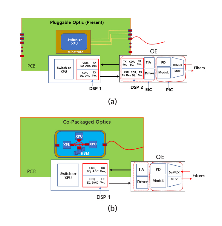

그림 5
광도파로에 대한 표면방출레이저 신호 전송 실험
출처 Reprinted from S.G. Park et al., “Technologies for optically interconnected CPU,” TechRxiv, 2022. doi: 10.36227/techrxiv.19738048.v1.

그림 6
광네트워크칩(Optical Network Chip) 모형도
출처 Reprinted from S.G. Park et al., “Technologies for optically interconnected CPU,” TechRxiv, 2022. doi: 10.36227/techrxiv.19738048.v1.

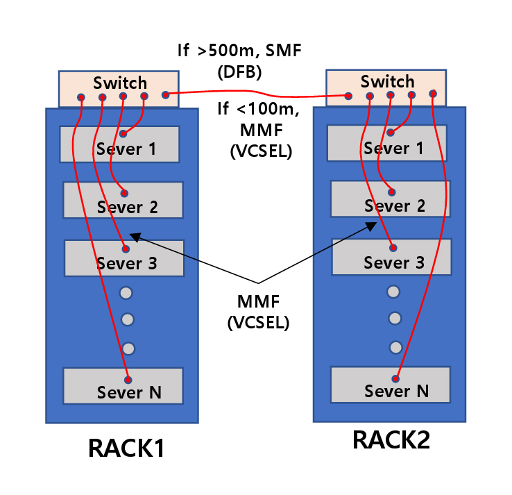


Figure 5
Transmission experiment of VCSEL light through optical waveguides.
Source: Reprinted from S.G. Park et al., “Technologies for optically interconnected CPU,” TechRxiv, 2022.

Figure 6
A conceptual diagram of an optical network chip
Source: Reprinted from S.G. Park et al., “Technologies for optically interconnected CPU,” TechRxiv, 2022.
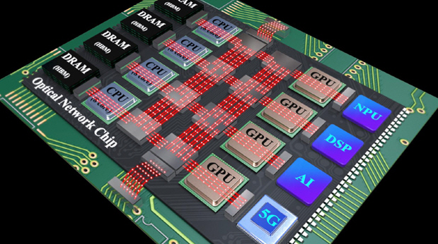
표 1 광트랜시버 기술 트렌드
| Pluggable on Board 2024 | CPO on Substrate 2026 | CPO on Chip 202x | |
|---|---|---|---|
| Bandwidth | 1.6Tb/s | 6.4Tb/s | 12.8Tb/s |
| Power | 1x | < 0.5x | < 0.1x |
| Latency | 1x | < 0.1x | < 0.05x |
표 2 실리콘포토닉스와 표면방출레이저 기반 광트랜시버 비교
표 3 광변조기의 최고 특성
| Si M-Z 변조기 | Si 링변조기 | |
|---|---|---|
| 3dB 밴드폭 변조속도 (PAM4) | 47GHz | 49GHz |
| 250Gb/s | 200Gb/s | |
| 소속 논문 | 캐나다, Mcgill U. PTL 2021[17] | 미국, HP사 Nature comm. 2024[18] |
| EML/DML | VCSEL | |
| 3dB 밴드폭 변조속도 (PAM4) | EML-65GHz | 멀티모드 30GHz |
| 225Gb/s | 224Gb/s | |
| DML-108GHz | 단일모드 39.4GHz | |
| 256Gb/s | 100Gb/s | |
| 소속 논문 | 일본, Mitsubishi, JLT 2024 [19] | 독일, VIS EL 2024[21] |
| 일본 NTT Nature Photon 2021[20] | 일본, 동경공업대 CLEO 2024[12] |
표 4 포토닉 인터포저 칩의 구성요소 및 특징
Table 1 Optical transceiver technology trend
| Pluggable on Board 2024 | CPO on Substrate 2026 | CPO on Chip 202x | |
|---|---|---|---|
| Bandwidth | 1.6Tb/s | 6.4Tb/s | 12.8Tb/s |
| Power | 1x | < 0.5x | < 0.1x |
| Latency | 1x | < 0.1x | < 0.05x |
Table 2 Comparison of silicon photonics and VCSEL-based optical transceivers
Table 3 Highest performances of optical modulators
| Si M-Z modulator | Si Ring modulator | |
|---|---|---|
| 3dB BW Modul. rate (PAM4) | 47 GHz | 49 GHz |
| 250 Gb/s | 200 Gb/s | |
| Affiliat. Publication | Canada, Mcgill U. | U.S., HP |
| PTL 2021 [17] | Nature comm. 2024 [18] | |
| EML/DML | VCSEL | |
| 3dB BW Modul. rate (PAM4) | EML-65 GHz | Multimode 30 GHz |
| 225 Gb/s | 224 Gb/s | |
| DML-108 GHz | Single M. 39.4 GHz | |
| 256 Gb/s | 100 Gb/s | |
| Affiliat. | Japan, Mitsubishi, JLT 2024 [19] | Germany, VIS EL 2024 [21] |
| Publication | Japan NTT Nature Photon 2021 [20] | Japan, T.I.T. CLEO 2024 [12] |
Table 4 Components and properties for photonic interposer chips
- Sign Up
- 전자통신동향분석 이메일 전자저널 구독을 원하시는 경우 정확한 이메일 주소를 입력하시기 바랍니다.